|
Electronic
Packaging Research
|
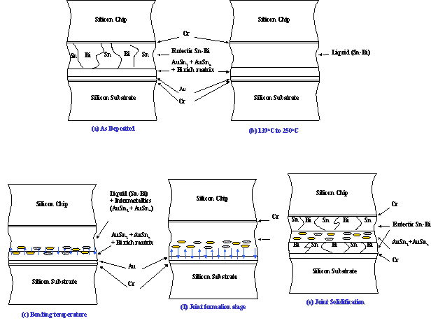
Bonding
principle of Bi/Sn/Au solder joints
|
|
|
Achieving high quality
fluxless solder joint in air ambient
Developing fluxless lead
free FCOF (flip chip on flex)
technology
Understanding
microstructure and phase formation of joints
Flip
chip packaging for high temperature and power devices
|
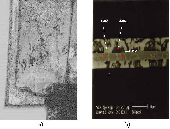
Solder
joints and Microstructure of Bi/Sn/Au
|
|
|
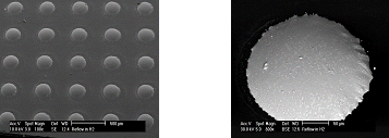
(a)
SAM acoustic image
of a Bi/Sn/Au solder joint
(b)
SEM image
of Bi/Sn/Au solder joint
Our
lab has transmission mode Scanning Acoustic Microscopy. Resolution: up
to 10micrometer
|
Fluxless
tin rich Au-Sn flip chip bonding process
|
|
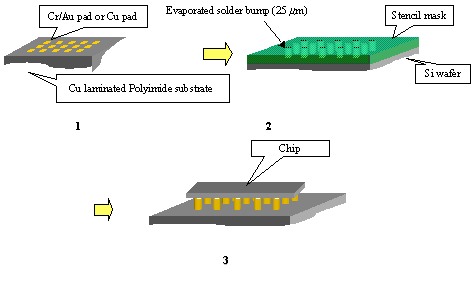
1.
Formation of Cr/Au pad
2.
Formation of solder bumps
through stencil mask on Si wafer
3.
Chip mounting and joint formation in
H2 ambient
|
|
|
|
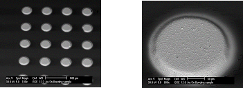
(a)
(b)
|
(a)
Multilayer tin rich eutectic Au-Sn bump after deposition
(b)
The tin rich eutectic Au-Sn solder bump after re-flow in hydrogen
|